Today's News: March 28
Second exam on Wednesday of next week.
Today is the last day to turn in Assignment 3.
Today is the last day to turn in Assignment 3.
This section deals with the design of hardware that makes up the basic building blocks of a computer.
Section 4.2.1: Logic Gates
The simplest building block we will discuss in this course is the gate.A gate has a small number of inputs (usually 1 or 2) and one output.
Logically, gates perform a Boolean function such as AND or OR.
Basic gate symbols:

In the old days, logic designer would draw diagrams based on these and similar gates to design a circuit.
Today, circuits are designed using a Hardware Description Language (HDL).
We will use a simple form of this called HCL (Hardware Control Language).
This looks very much like C code.
For example, an And gate is represented by a && b.
Sections 4.2.2 - 4.2.4: Combinational Circuits
Example: bit equalbool eq = (a && b) || (!a && !b);
This is equivalent to the following circuit:

Here is an alternate way of showing the same circuit:

Here is a block diagram:

We can make a multi-bit equal out of 1-bit equals:
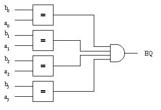
And here is a block diagram:

Equals Circuit
Example: 1-bit multiplexer
It allows you to select one of two one-bit inputs and is described by
bool out = (s && a) || (!s && b);

Here is a block diagram:

We can make a multi-bit (word level) mux out of 1-bit muxes:

Here is a block diagram for this:

Here is the HCL description of the mux:
int Out = [
   s: A;
   1: B;
];
The [...] is like a select, it means if s is true, the result is A.
Otherwise, we check the next case. 1 is always true, so we select B.
Today's News: March 31
Second exam on Wednesday of this week.
Question:
In the 2-input mux described above, which input is selected when s=0?
Answer:
You can also make a mux that selects from more than 2 words.
Here is a 4 word mux, called a 4-way mux:

Here is the HCL description of the 4 word mux:
int Out4 = [
   !s1 && !s0: A;
   !s1       : B;
   !s0       : C;
   1         : D;
];
Question:
In the 4-input mux described above, if s1s0 is considered a 2-bit binary number
with s0 as the low order bit, which input is selected by each of the s-values: 0, 1, 2, and 3?
Answer:
The diagrams and HCL for the 2-input and 4-input muxes were taken from the textbook.
Note the inconsistency as to the order of the inputs.
In one of the diagrams, the smallest value of s selects the top input and in the other the smallest value of s selects the bottom number.
Multiplexers 1
Other Gates and Basic Building Blocks
This is not in the book.Another common gate is the XOR:

which is the same as

Any circuit that can be made from and, or and not gates can also be made just using and and not because:
a || b = !(!a && !b);
Similarly, you can use just or and not:
a && b = !(!a || !b);
These pairs (and, not) and (or, not) are called functionally complete sets.
Problem:
Show that and alone is not a functionally complete set.
Are there any single gates that can be used as a functionally complete sets? Yes!
The NAND Gate:
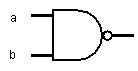
The NOR Gate:

Two input gates
Adders
This is not in the book. Some diagrams are from Wikipedia.It is easy to design a 1 bit adder that has 2 inputs and 2 outputs:

This is called a half adder.
Today's News: April 4
Exam 2 returned today.
We could make a 2-bit adder from this, but it would be more convenient to make it from full adders, which add 3 bits.

Here is a block diagram of a 1-bit full adder:
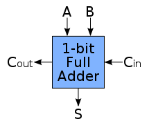
You can use this to make a 4-bit full adder which takes as input two 4-bit numbers and a carry coming in and produces 5 bits of output.

This is called a ripple carry adder. Each successive adder cannot produce the correct output until the previous carry is produced.
How could you make a 16-bit adder from four 4-bit adders?
Problem: Design a word level subtracter.
Adder Gate Count
Today's News: April 7
Propagation Delay
This is not in the book - diagrams are from Wikipedia.- Real gates are made from transistors and instead of using Boolean values true and false (or 0 and 1), voltages are used.
- A voltage greater than a true-threshold is true, and a voltage less than a false-threshold is false. (Or interchange greater and less.)
- Voltages between these two thresholds give undefined results.
- When you change an input, it takes some time, called the propagation delay, or gate delay, for the output voltage to reach its correct value.
- This delay is additive as you go through a circuit, and the total delay is determined by the longest path.
- The propagation delay determines how fast your CPU can run.

There are three gate delays to produce the carry, and only 2 to produce the sum.
However, there are only 2 gate delays from the carry in to the carry out.
If we have a 4-bit ripple carry adder, the first carry requires 3 gate delays and each additional level is 2 gate delays, for a total of 9 gate delays.
Note: We are assuming (incorrectly) that the propagation delay is the same for all gates and we are ignoring the propagation delay of the wires.
Question:
A processor runs at 3 GHz and requires that all propagation delays are less than 1/3 of a nanosecond.
Estimate the length of a wire that would produce a 1/3 nanosecond delay.
Answer:
Estimate the length of a wire that would produce a 1/3 nanosecond delay.
Important fact: in theory, any boolean function can be created using only 2 gate delays (not counting inverters).
This can be done with a 2-level AND-OR network or a 2-level OR-AND network.
Explanation 1:
The rules of Boolean algebra allow you to write any Boolean function of 2 variables, a and b in the form:
f(a,b) = c0a'b' + c1a'b + c2ab' + c3ab
Where the c's are either 0 or 1 and a' = !a, and b' = !b, and we use + for OR and
multiplication for AND.
Similarly, any Boolean function of 3 variables can be written as a combination of a'b'c', a'b'c, ab'c', etc.
Example:
s = f(a,b) = (a ^ b) ^ c
Using X ^ Y = X'Y + XY', we get
s = f(a, b) = (a'b + ab')'c + (a'b + ab')c'
            = ((a'b)'(ab')')c + a'bc + ab'c
            = (a + b')(a' + b)c + a'bc + ab'c
            = (aa' + ab + b'a' + b'b)c + a'bc + ab'c
            = abc + b'a'c + a'bc' + ab'c'
This is just the calculation of the sum for the 1-bit full adder.
Note that all it says is that the sum is true if the number of true inputs is 1 or 3.
Explanation 2:
Any Boolean function can be described by a truth table. Let us look at the truth table for the calculation of the sum of a one-bit full adder:
| a | b | cin | s |
| 0 | 0 | 0 | 0 |
| 0 | 0 | 1 | 1 |
| 0 | 1 | 0 | 1 |
| 0 | 1 | 1 | 0 |
| 1 | 0 | 0 | 1 |
| 1 | 0 | 1 | 0 |
| 1 | 1 | 0 | 0 |
| 1 | 1 | 1 | 1 |
s = a'b'c + a'bc' + ab'c' + abc
Here is the corresponding 2-level AND-OR network:

We can do something similar with the carry out of a 1-bit full adder, but it is simpler to get a formula by noting that there is a carry if at least two of the three inputs are 1:
cout = ab + ac + bcand the circuit looks like this:

Two Level Adder
It is possible to produce similar formulas for the other 3 carries of a 4-bit full adder and put them into a circuit that will create all carries with 2 gate delays.
If all carries are produced with 2 gate delays so that sums are produced 2 gate delays later. Total gate delays for the 4-bit adders: 4 instead of 9. It is more than twice as fast!
For a 64-bit adders, a ripple carry adder would have 129 gate delays. If all carries are produced with 2 gate delays, the sums are produced 2 gate delays later. Total gate delays for a 64-bit adder: 4 instead of 129. It is more than 30 times faster.
In practice, this is not feasible for 32-bit or 64-bit adders.
There are limitations based on the number of inputs a gate can have and on how many inputs can be driven by a single output.
A fast adder might look like the diagram below for a 4-bit carry lookahead adder:

The p and g outputs of the full adder are independent of the carry and are available after 2 gate delays.
All of the carries are generated 2 gate delays later.
The PG and PP outputs are available at about the same time and allow nesting of the logic so that C8, C12, C16 can be available about 2 gate delays later.
It allows for a design of an n-bit adder with a propagation delay proportional to log n instead of n.
Wikipedia has a good discussion of the details.
The ALU
An Arithmetic/Logic Unit is a circuit that can produce one of several arithmetic (add, subtract, etc.) or logical (and, or, etc.) functions.
The Y86 will need an ALU that can add, subtract, and, and xor.
Basically, this ALU would be designed like this:

Here is a block diagram of this ALU:

Today's News: April 9
Sections 4.2.5: Memory and Clocking
Note: Most of this is not in the text.So far we have talked about combinational circuits.
These must follow certain rules such as
- Outputs of two logical gates cannot be connected together.
- The network must be acyclic:
There cannot be a path that loops back upon itself.
If we relax this constraint, we can get something like the diagram below which is called an SR latch.
It is a basic building block of a memory circuit.
The SR Latch
.svg.png)
Note that the output of a NOR gate is only 1 if both inputs are 0.
Another way of saying this is that if either input is 1, the output is 0.
Let us try to make a truth table for this network:
Three cases are easy:
- if R is 1 and S is 0:
the output of the upper gate is 0, so Q = 0
both inputs of the lower gate are 0, the output of the lower gate is 1, so Q-bar is 1. - if R is 0 and S is 1:
the output of the lower gate is 0, so Q-bar = 0
both inputs of the upper gate are 0, so Q = 1 - if R and S are both 1:
the output of both gates are 0, so Q-bar = 0 and Q = 0.
if R and S are both 0, 2 cases:
- If the other input to the upper gate is 0, Q-bar = 0 and Q = 1.
- If the other input to the upper gate is 1, Q-bar = 1 and Q = 0.
How we use the SR Latch:
- Never let R and S be 1 simultaneously.
Under these conditions, Q-bar is the complement of Q. - Making R = 1 and then returning it to 0, resets the latch so that Q = 0.
- Making S = 1 and then returning it to 0, sets the latch so that Q = 1.
The SR Latch is an example of a sequential circuit.
Such a circuit can have outputs that depend on the past history of its inputs.
Sequential circuits are said to have state or memory.
Combinational circuits have outputs that depend only on the current values of the inputs.
Combinational circuits do not have any memory.
A more useful device is the D Latch.
It adds a few gates to the front end of the SR latch so it cannot be in the state with R and S both 1:
The D Latch
-Labeled.svg.png)
Note that R and S cannot both be true.When E is true, S=D and R=D', so Q = D.
When E is false, R=S=0, and the RS latch stores its value: changes to D do not affect Q.
Question:
Why are the inputs called D and E?
Answer:
Here is the block diagram for the D Latch:

D Latch
Notice the pattern we are using to do our hardware design:
- Design a circuit from known components.
- Understand how it works.
- Understand what it does.
- Use a block diagram to represent the circuit.
- We now only need to remember what the circuit does and can forget about how it works (until an exam).
Today's News: April 11
The D latch is a device with an enable input.
The idea of an enable input is that the data in the latch can only change when the enable input is true.
What we really want is a clocked circuit.
This stores its input only when the clock input changes from low to high (or vice versa).
It can be made by putting two latches together.
One way to do this is to allow the first latch to change only when the clock is high, and the second to change only when it is low.
Here is a diagram of a D flip-flop that is clocked when the input becomes negative.
The D Flip Flop
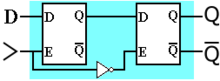
When the clock input becomes high, the first latch (the master) stores the value
of D.
The second latch cannot change because its E input is low.
When the clock becomes low, the slave latch stores the value from the master.
As long as the clock stays low, the master cannot change, so the slave also cannot change (even though it is enabled).
By changing the position of the inverter, we can make the outputs change when the clock becomes high.
Here is a block diagram for the positive edge triggered D flip flop.

When the clock input becomes high (positive edge triggered), the value of D is stored in the flip flop.
This is the building block for a multi-bit register.
D FLip Flop
The Register File
Putting putting several multi-bit registers together with a mux, we can make a register file.
Here is the block diagram of a register file:

When the clock goes high, the valW value is stored in the register with address dstW.
At any time we can read the values of two of the registers in the register file.
The srcA input to determines which register is available at the valA outputs.
The srcB input to determines which register is available at the valB outputs.
These are independent of the clock.
If you change the read inputs, the corresponding outputs will change after some propagation delay.
Register File Design
Random access memory can be done in a similar way, but usually is done with different technology since this is expensive and uses a lot of power.